Abstract: Chalcogenide phase change materials (PCMs) have promising properties for photonic applications thanks to their nonvolatile and large refractive index modulation [1]. The last decade has seen a growing interest in such a combination of properties for a variety of nonvolatile programmable devices, such as metasurfaces, tunable filters, phase/amplitude modulators, color pixels, thermal camouflage, photonic memories/computing, plasmonics, etc.—giving rise to the so-called Phase-change Photonics field.[1] PCM-based devices rely on the precise switching between the amorphous and the crystalline states, which can be achieved through optical or electrical pulses via optical absorption and Joule heating, respectively. Optical pulse switching is the fastest and most precise method; however, it lacks scalability given the difficulty of on-chip pulse routing when considering many PCM cells. It is also limited to absorptive PCMs, such as Ge2Sb2Te5. As a scalable alternative, on-chip microheaters using multiple material platforms have been proposed, e.g. doped-silicon, graphene, ITO, metals, etc. Doped-silicon microheaters are particularly interesting since they are CMOS compatible and can be fabricated onto silicon-on-insulator (SOI) wafers—the same platform used for silicon photonic integrated circuits. However, this electro-thermal switching also has shortcomings. It lacks stable multi-level response due to the stochastic nature of both amorphization and crystallization processes in the typical bow-tie-like devices where the microheater heats the entire cell to an almost flat temperature [2,3]. Because of this, the focus is shifting towards the microheater’s geometry in addition to the choice of conductive material and its integration. One common goal is to control the hotspot size within the PCM cell to deterministically switch specific areas (i.e., spatially resolved amorphous domains in a crystalline cell) and, thus, achieve controllable and reproducible optical modulation [4,5]. In this talk, I will review the fundamentals of PCM for photonics and the proposed electro-thermal mechanisms. I will then focus on our current efforts to re-engineer doped-silicon microheaters for optimum performance.
[1] M. Wuttig, et, al. “Phase-change materials for non-volatile photonic applications,” Nat. Photon.11(8), 465–476 (2017).
[2] J. Feldmann, et, al. “Calculating with light using a chip-scale all-optical abacus,” Nat Commun 8(1), 1256 (2017)
[3] T. Tuma, et, al. “Stochastic phase-change neurons,” Nat. Nanotechnol.11(8), 693–699 (2016).
[4] C. Ríos, et, al “Ultra-compact nonvolatile phase shifter based on electrically reprogrammable transparent phase change materials,” PhotoniX 3(1), 26 (2022).
[5] X. Li, et, al, “Fast and reliable storage using a 5 bit, nonvolatile photonic memory cell,” Optica 6, 1-6 (2019)
[6] Y. Zhang, et, al, “Myths and truths about optical phase change materials: A perspective.” Appl. Phys. Lett. 118 (21): 210501.
Biographical Sketch: Carlos A. Ríos Ocampo is an Assistant Professor at the University of Maryland, College Park, where he has led the Photonic Materials & Devices groups since 2021. Before joining UMD, Carlos was a Postdoctoral Associate at MIT, received a DPhil (PhD) degree in 2017 from the University of Oxford (UK), an MSc degree in Optics and Photonics in 2013 from the KIT (Germany), and a BSc in Physics in 2010 from the University of Antioquia (Colombia). Carlos’s scientific interests focus on studying and developing new on-chip technologies driven by the synergy between nanomaterials and photonics.


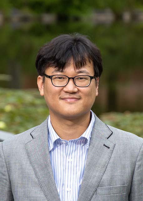

 Abstract: Recent decades have seen rapid development in all manufacturing technologies, including additive manufacturing (AM). This has raised the need for design methods to leverage the new, increasingly complex fabrication possibilities. Topology optimization has the potential to generate new high-performing design solutions since it is a free-form design method that does not require a preconceived notion of the final layout. It uses computational mechanics and optimization tools to generate improved designs. For operating designs to perform as predicted, the used model must capture the material behavior. Additionally, the planned manufacturing process might induce material characteristics and design limitations that should be considered as the design is generated. This talk focuses on identifying and incorporating behavioral and manufacturing aspects within the design process. Different strategies for integration within topology optimization will be discussed. This includes consideration of manufacturing-induced material characteristics, which is illustrated through tailoring design to material extrusion-based AM. In material extrusion, a nozzle moves across a build plate and deposits a material bead on a 2D slice of the design. These processes typically induce some degree of anisotropy through weak(er) bonding between adjacent beads. To improve the manufacturability of large-scale designs, the application of a Mixed Integer Linear Programming formulation is discussed for highly restricted volume scenarios. Finally, a new design framework is introduced in which the interactive participation of the design engineer is enabled to resolve more complex mechanic phenomena.